Nanoscale Characterisation & Processing |
|
Main Navigation
|
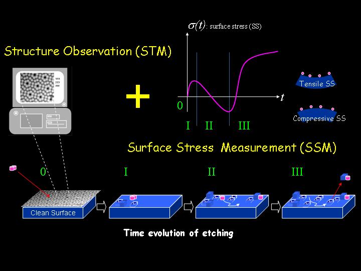
Origins and Atom-Scale Measurement of Surface Stress Unlike metals, semiconductors are unable to effectively screen charge. An important consequence of this is that when during a surface chemical reaction bonds become strained and the strain field produced locally accumulates across the surface as the reaction proceeds. Using long, ultra-thin samples we have demonstrated that the resulting surface stress can be measured by the deflection of the sample between the plates of a parallel capacitor. To identify the surface species that are actually responsible for this behavior we have incorporated an STM into the surface stress measurement (SSM) system. We have also incorporated a strain stage in this system that allows us to mechanically induce a surface stress and then to determine its influence on surface chemical reactivity. At present, we are studying the role of simple steric interactions on Si that induce compressive stress, such as halogen adsorbates that are typically used in chemical etching. In the case of halogens on Si(111) we have been able to identify various stages in the reaction where the surface shifts from being globally compressive to tensile and visa-versa, and to relate these changes to particular chemical reactions. In addition we are studying the growth of strained over-layers such as Ge on Si(100), which is used to engineer the band-gap in high performance transistors and stress induced by ion-sputtering.
Real-time and In-situ Surface Stress and STM Measurements |