Nanoscale Characterisation & Processing |
|
Main Navigation
|
Nanoscale Electrical Transport Measurements: An understanding of the transport properties of nanoscale assemblies is essential for the development of nanoscale devices. There are two aspects to this problem that are of particular interest. The first, involves the properties of nanowires, and how to best to form contacts with these systems so as to measure transport. We are exploiting the use of a dual focused-ion-beam/scanning-electron-microscope for beam induced deposition of a metal from a precursor gas to form contacts, as well as writing contacts using e-beam lithography, followed by contact metal deposition and lift-off. Nanowire systems are then characterized by the 4-probe method performed over a range of temperatures (5K – 800K). Temperature studies are important as 1-d nanowire systems are prone to undergoing metal-to-insulator transitions that are influenced by interactions with other wires and even attached molecules. Our goal is to understand why these transitions occur in some systems and not others and how this phenomenon can be used for device applications. The second area of interest is the establishment of contacts using self-assembly techniques. In this case the recognition chemistry remains in the contact region, and we are interested in its influence in the transport properties of the assembly. Depending on the nature of the recognition chemistry these pinned molecules may impart novel properties to the assembly. In the instance where their influence is unwanted, we are interested in developing post-assembly processing techniques that enable the molecules to be degraded in a manner that produces useful contacts.
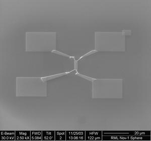
Fig. 1. An electrode array defined by beam induced deposition of Pt.
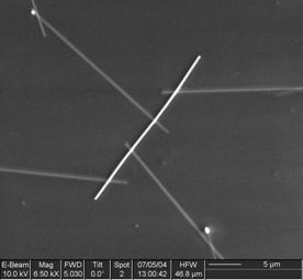
Fig 2 & 3. LiMo 3Se 3 nanowires with four Pt electrodes.
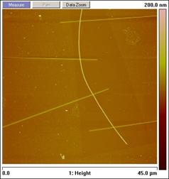
Fig 4. In-situ manipulation of a gold nanowire onto an electrode array.
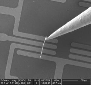
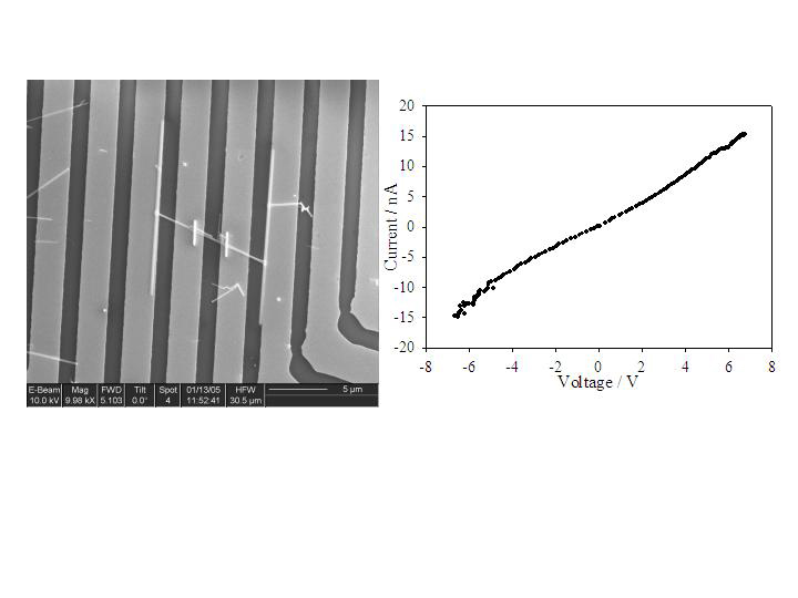
Fig 5. Right: SEM image of 150 nm diameter B-doped Si NW, pinned to the Au contacts by Pt lines deposited by e-beam (inner contacts) and ion beam (outer contacts).Left: 4-point IV measurement of the wire shown on the right. This gives a resisitivty of 2.4 W m. |